- 您现在的位置:买卖IC网 > Sheet目录342 > MCBSTM32EXL (Keil)BOARD EVALUATION FOR STM32F103ZE
�� �
�
�RM0008�
�Advanced-control� timers� (TIM1&TIM8)�
�For� example,� you� can� measure� the� period� (in� TIMx_CCR1� register)� and� the� duty� cycle� (in�
�TIMx_CCR2� register)� of� the� PWM� applied� on� TI1� using� the� following� procedure� (depending�
�on� CK_INT� frequency� and� prescaler� value):�
�●�
�●�
�●�
�●�
�●�
�●�
�●�
�Select� the� active� input� for� TIMx_CCR1:� write� the� CC1S� bits� to� 01� in� the� TIMx_CCMR1�
�register� (TI1� selected).�
�Select� the� active� polarity� for� TI1FP1� (used� both� for� capture� in� TIMx_CCR1� and� counter�
�clear):� write� the� CC1P� bit� to� ‘0’� (active� on� rising� edge).�
�Select� the� active� input� for� TIMx_CCR2:� write� the� CC2S� bits� to� 10� in� the� TIMx_CCMR1�
�register� (TI1� selected).�
�Select� the� active� polarity� for� TI1FP2� (used� for� capture� in� TIMx_CCR2):� write� the� CC2P�
�bit� to� ‘1’� (active� on� falling� edge).�
�Select� the� valid� trigger� input:� write� the� TS� bits� to� 101� in� the� TIMx_SMCR� register�
�(TI1FP1� selected).�
�Configure� the� slave� mode� controller� in� reset� mode:� write� the� SMS� bits� to� 100� in� the�
�TIMx_SMCR� register.�
�Enable� the� captures:� write� the� CC1E� and� CC2E� bits� to� ‘1’� in� the� TIMx_CCER� register.�
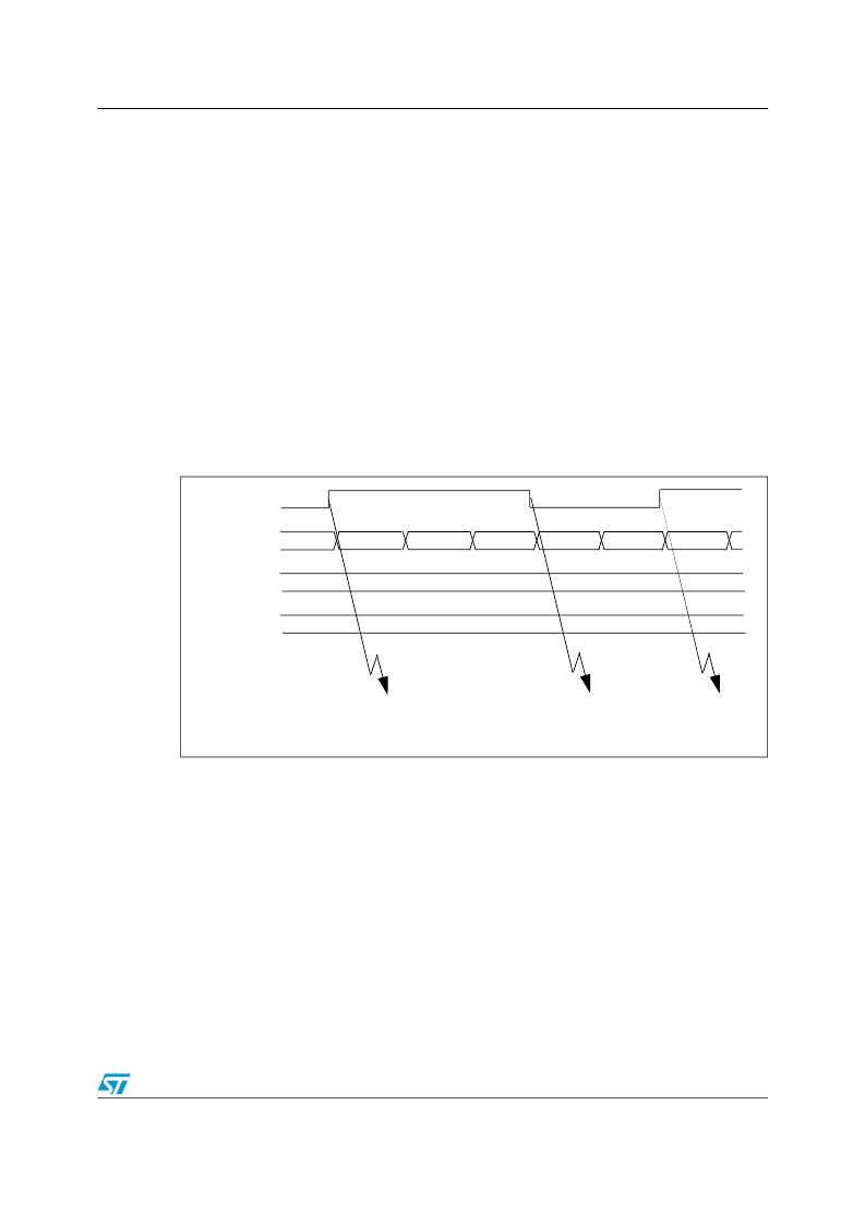
�Figure� 81.� PWM� input� mode� timing�
�TI1�
�TIMx_CNT�
�0004�
�0000�
�0001�
�0002�
�0003�
�0004�
�0000�
�TIMx_CCR1�
�TIMx_CCR2�
�0004�
�0002�
�IC1� capture�
�IC2� capture�
�reset� counter�
�IC2� capture�
�pulse� width�
�measurement�
�IC1� capture�
�period�
�measurement�
�ai15413�
�1.� The� PWM� input� mode� can� be� used� only� with� the� TIMx_CH1/TIMx_CH2� signals� due� to� the� fact� that� only�
�TI1FP1� and� TI2FP2� are� connected� to� the� slave� mode� controller.�
�13.3.8�
�Forced� output� mode�
�In� output� mode� (CCxS� bits� =� 00� in� the� TIMx_CCMRx� register),� each� output� compare� signal�
�(OCxREF� and� then� OCx/OCxN)� can� be� forced� to� active� or� inactive� level� directly� by� software,�
�independently� of� any� comparison� between� the� output� compare� register� and� the� counter.�
�To� force� an� output� compare� signal� (OCXREF/OCx)� to� its� active� level,� you� just� need� to� write�
�101� in� the� OCxM� bits� in� the� corresponding� TIMx_CCMRx� register.� Thus� OCXREF� is� forced�
�high� (OCxREF� is� always� active� high)� and� OCx� get� opposite� value� to� CCxP� polarity� bit.�
�For� example:� CCxP=0� (OCx� active� high)� =>� OCx� is� forced� to� high� level.�
�The� OCxREF� signal� can� be� forced� low� by� writing� the� OCxM� bits� to� 100� in� the� TIMx_CCMRx�
�register.�
�Doc� ID� 13902� Rev� 9�
�273/995�
�发布紧急采购,3分钟左右您将得到回复。
相关PDF资料
MCBTMPM330
BOARD EVAL TOSHIBA TMPM330 SER
MCIMX25WPDKJ
KIT DEVELOPMENT WINCE IMX25
MCIMX53-START-R
KIT DEVELOPMENT I.MX53
MCM69C432TQ20
IC CAM 1MB 50MHZ 100LQFP
MCP1401T-E/OT
IC MOSFET DRVR INV 500MA SOT23-5
MCP1403T-E/MF
IC MOSFET DRIVER 4.5A DUAL 8DFN
MCP1406-E/SN
IC MOSFET DVR 6A 8SOIC
MCP14628T-E/MF
IC MOSFET DVR 2A SYNC BUCK 8-DFN
相关代理商/技术参数
MCBSTM32EXLU
功能描述:开发板和工具包 - ARM EVAL BOARD + ULINK2 FOR STM32F103ZG
RoHS:否 制造商:Arduino 产品:Development Boards 工具用于评估:ATSAM3X8EA-AU 核心:ARM Cortex M3 接口类型:DAC, ICSP, JTAG, UART, USB 工作电源电压:3.3 V
MCBSTM32EXLU-ED
制造商:ARM Ltd 功能描述:KEIL STM STM32EXL EVAL BOARD
MCBSTM32EXLUME
功能描述:开发板和工具包 - ARM EVAL BOARD + ULINKME FOR STM32F103ZG
RoHS:否 制造商:Arduino 产品:Development Boards 工具用于评估:ATSAM3X8EA-AU 核心:ARM Cortex M3 接口类型:DAC, ICSP, JTAG, UART, USB 工作电源电压:3.3 V
MCBSTM32F200
功能描述:开发板和工具包 - ARM EVAL BOARD FOR STM STM32F207IG
RoHS:否 制造商:Arduino 产品:Development Boards 工具用于评估:ATSAM3X8EA-AU 核心:ARM Cortex M3 接口类型:DAC, ICSP, JTAG, UART, USB 工作电源电压:3.3 V
MCBSTM32F200U
功能描述:开发板和工具包 - ARM EVAL BOARD FOR STM STM32F207IG + ULINK2
RoHS:否 制造商:Arduino 产品:Development Boards 工具用于评估:ATSAM3X8EA-AU 核心:ARM Cortex M3 接口类型:DAC, ICSP, JTAG, UART, USB 工作电源电压:3.3 V
MCBSTM32F200UME
功能描述:开发板和工具包 - ARM EVAL BOARD FOR STM STM32F207IG ULINK-ME
RoHS:否 制造商:Arduino 产品:Development Boards 工具用于评估:ATSAM3X8EA-AU 核心:ARM Cortex M3 接口类型:DAC, ICSP, JTAG, UART, USB 工作电源电压:3.3 V
MCBSTM32F200UME-ED
制造商:ARM Ltd 功能描述:KEIL STM32F207IG EVAL BOARD
MCBSTM32F400
功能描述:开发板和工具包 - ARM EVAL BOARD FOR STM STM32F407IG
RoHS:否 制造商:Arduino 产品:Development Boards 工具用于评估:ATSAM3X8EA-AU 核心:ARM Cortex M3 接口类型:DAC, ICSP, JTAG, UART, USB 工作电源电压:3.3 V